The EU Chips Act came into force in September 2023. Since then, many EU countries have supported the establishment of semiconductor production facilities. Germany, Poland and Lithuania have successfully launched new projects through international partnerships with US or Taiwan market leaders Intel and TSMC. Europe, like the US, aims to achieve independence from China in the semiconductor industry.
Sandy Chou
2 April 2024
Arabic version | Chinese version | French version | German version
To achieve strategic autonomy in the semiconductor industry, the EU Commission began developing its Chips Act in 2022. The EU Chips Act came into force on 21 September 2023, but even before then, several European governments accelerated investment into their domestic chip industries. 80% of global chip production is based in Asia with the Taiwan Semiconductor Manufacturing Company (TSMC) being the world’s largest independent semiconductor foundry. By 2030 the EU wants to double its chip production to 20% of the global market.
In August 2023, TSMC announced construction of a chip foundry in Dresden, Germany, under the auspices of a new company, the European Semiconductor Manufacturing Company (ESMC). Seventy percent of this new entity is owned by TSMC, and the remaining thirty percent by several German manufacturing companies, including Bosch, NXP, and Infineon.
ESMC’s production of chips, expected to begin in 2027, will help fulfill a main goal of the EU Chips Act – independent production and an uninterruptable supply of microchips for various industries. The Dresden ‘fab’ (a term used to refer to any semiconductor fabrication facilities), is expected to attract more vendors and investment for Germany and its neighboring countries, due to the cluster effect it will create in the industry, i.e. the synergies and cost savings achieved by businesses located in close proximity. This effect is more pronounced for semiconductor fabs than for traditional manufacturing factories. While suppliers inevitably move closer to the fab in order to facilitate the fabrication and distribution of chips, the semiconductor cluster effect also tends to encourage establishment of a science park or campus, which in turn further stimulates the economy around it.
In early 2023, Intel, the largest chip integrated device manufacturer (IDM) in the world, finalized its fab investment in Magdeburg, Germany. Total investment to build the Magdeburg facility is EUR 30 billion, with the German government providing subsidies of EUR 10 billion. Intel and the German government are investing into an entire chips’ ecosystem and the future of EU chips independence. This investment has not been without criticism. Economists are doubting the decision by the German government pointing out that these 3000 newly created jobs will end up costing EUR 3 million per workplace. Those in support of the government’s strategic investment decision argue that the new European ESMC and Intel fabs, will ensure EU independence in the semiconductor supply chain in the future.
Only a few months after the ESMC deal, Poland announced a joint venture with Intel to build a plant in Wrocław devoted to advanced chip packaging. “Advanced Packaging” is a process that integrates the functions of individual chip elements within a single chip, and requires high levels of expertise. This process is crucial for the manufacture of high-performance computing chips that are critical for artificial intelligence (AI).
The explosive demand for AI chips has been a major trend since 2023. The packaging plant in Wrocław is likely to build strategic alliances with other partners, such as advanced packaging companies in Taiwan or Japan. The plant will primarily engage in packaging for Intel chips made in Magdeburg, but will also take packaging orders from other fabs. An advanced chip packaging plant in Europe has the potential to reduce overseas packaging requirements, centralization of the supply chain, and thus enhance European competition and independence in global markets.


As one of the first European countries to cooperate with Taiwan in a technology exchange, Lithuania is another EU member state entering into an international partnership in the semiconductor industry. Laser technology is crucial in manufacturing tools and Lithuania exchanged its expertise in lasers for Taiwan’s patents related to 8-inch wafer technology. Lithuania can now build a foundry based on 8-inch wafers, and this, along with its advance laser technology, is expected to enhance the yield rate of chip production. A high yield rate indicates a chip-maker has high production efficiency and low production cost, which in turn increases customer trust and brings additional business opportunities.
While creativity-driven organizations with intellectual property (IP) rights for chips technology and specializing in integrated circuit design are vital to the US and Canada chips industry, some US semiconductor companies are experiencing challenges in high-tech manufacturing. The Biden Administration has made the semiconductor industry a top priority, pledging to subsidize new foundries with USD 50 billion and invest an extra USD 200 billion into R&D. In the US, Intel will receive USD 8.5 billion in subsidies and USD 11 billion in special loans. The US, like the EU, aims to control 20% of the semiconductor industry moving forward.
In the near future, the most highly anticipated chip breakthroughs will likely occur in three areas: 1.) the development of technology required in quantum chips used for high performance computing; 2.) the production of even thinner chips; and 3.) the enhancement of packaging technology for AI chips. Given the interconnectivity of the technologies involved in the microchip industry, any country wishing to break into the market or continue to stay ahead of its competitors must identify the missing components in production and/or the supply chain, as well as create a long-term plan that involves cooperation with allies.
Although several European organizations are working with partners outside Europe, it is too early to tell whether Europe’s independent chip production will evolve into a dominant global market share. The key to success will depend on whether there are further breakthroughs in advanced packaging technology, continuous human resources devoted to this field and a business model that cleverly uses geopolitical factors in the industry.
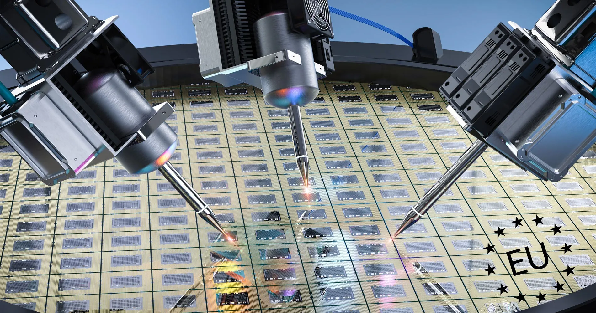
Picture: Semiconductor manufacturing with robotic arms. © PhonlamaiPhoto@Canva
More Articles on the EU Chips Act:
EU Chips Act to Boost EU Security and Semiconductor Manufacturing